取り扱いの注意
製品取り扱い上の注意事項(標準仕様)/ Precautions On Handling (Standard)
1. 保 管/Storage
保管は高温、多湿、長期保存を避けて常温常湿のもとで開封後は直ちに実装して下さい。
To store products it is recommended to avoid high temperature, high humidity and a long-term preservation.
Immediate mount is strongly recommended when products are exposed under normal temperature.
2. 電源のバイパスコンデンサー/Bypass capacitor of power supply
本製品使用の際は、電源とGND間に0.01μF程度のバイパスコンデンサーを入れて下さい。
It is recommended to put a 0.01μF bypass capacitor in between power supply and GND.
3. 静電気の影響/Influence of static electricity
本カタログ品には、C-MOS ICを使用しておりますので静電気対策をされ、過電圧に対する注意をお願いいたします。
Since C-MOS IC is used for products in this catalog, counter measures for static electricity and over voltage are recommended.
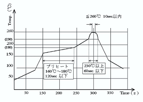
4. はんだ付け条件(リフロー)/Soldering conditions (Reflow)
温度上昇は可能な限り緩やかな勾配にして260℃以下で10秒以内、通過回数2回までとして下さい。
It is recommended to make the heat rise slope as moderate as possible and to limit the passage to 2 times within 10 seconds at temperature below 260 degrees.
5. 衝 撃/Impact
水晶製品実装後に基板を誤って落としたり、過度の衝撃、振動を与えた場合は、必ず特性の確認を行って下さい。
自動実装、チップマウンター等をご使用の際は水晶製品に加わる衝撃を抑えるように設定して下さい。
It is strongly recommended to reconfirm the features when the board is accidentally dropped after crystal Products are mounted or strong shocks and/or vibration is given. When automatic mounters and chip mounters are used measures for softening impacts to crystal products are recommended.
6. 基板曲げによるストレス/Stress by substrate bends.
極端な基板の変形はパターン剥がれ、製品電極剥がれ、はんだの亀裂や製品パッケージの損傷となり、性能劣化や誤動作の原因になる場合がありますので、特に実装後に基板を小割りにする場合は十分ご注意願います。
Since extreme distortion of the board causes pattern peeling, electrodes’ peeling, solder cracks, damages to a product package, etc., and eventually causes a bad performance and a wrong operation.
Therefore, it is recommended to pay an attention when a board splits into small pieces after mounting.
* 超音波、振動等を応用した使用については製品損傷の恐れが生じますのでご使用の際は、予めご確認願います。
* Prior confirmation is recommended to use an ultrasonic wave, vibrations, etc, since the product could be damaged.